LDO Design
Overview
The LDO module in the LDO_AC3E repository provides a low-dropout voltage regulator designed to maintain a stable output voltage despite fluctuations in the input voltage.
Parameters
Dropout Voltage: The minimum voltage difference between the input and output required for the LDO to operate properly.
PSRR (Power Supply Rejection Ratio): The ratio of change in output voltage to change in input voltage, indicating how well the LDO rejects changes in the input voltage.
Quiescent Current: The current consumed by the LDO when there is no load.
Line Regulation: The ability of the LDO to maintain a constant output voltage despite changes in the input voltage.
Load Regulation: The ability of the LDO to maintain a constant output voltage despite changes in the load current.
Phase Margin: The difference in phase between the LDO’s output and input signals at the unity gain frequency, indicating stability.
Open-Loop Gain: The gain of the LDO without feedback, often characterized in dB or decibels.
Topology
The Low Dropout Regulator (LDO) in use employs an operational transconductance amplifier (OTA) in conjunction with a PMOS pass transistor. The OTA compares a reference voltage with the output voltage feedback, generating an error signal to control the conductance of the pass transistor. This setup maintains a stable output voltage despite input voltage variations, making it ideal for low-power applications.
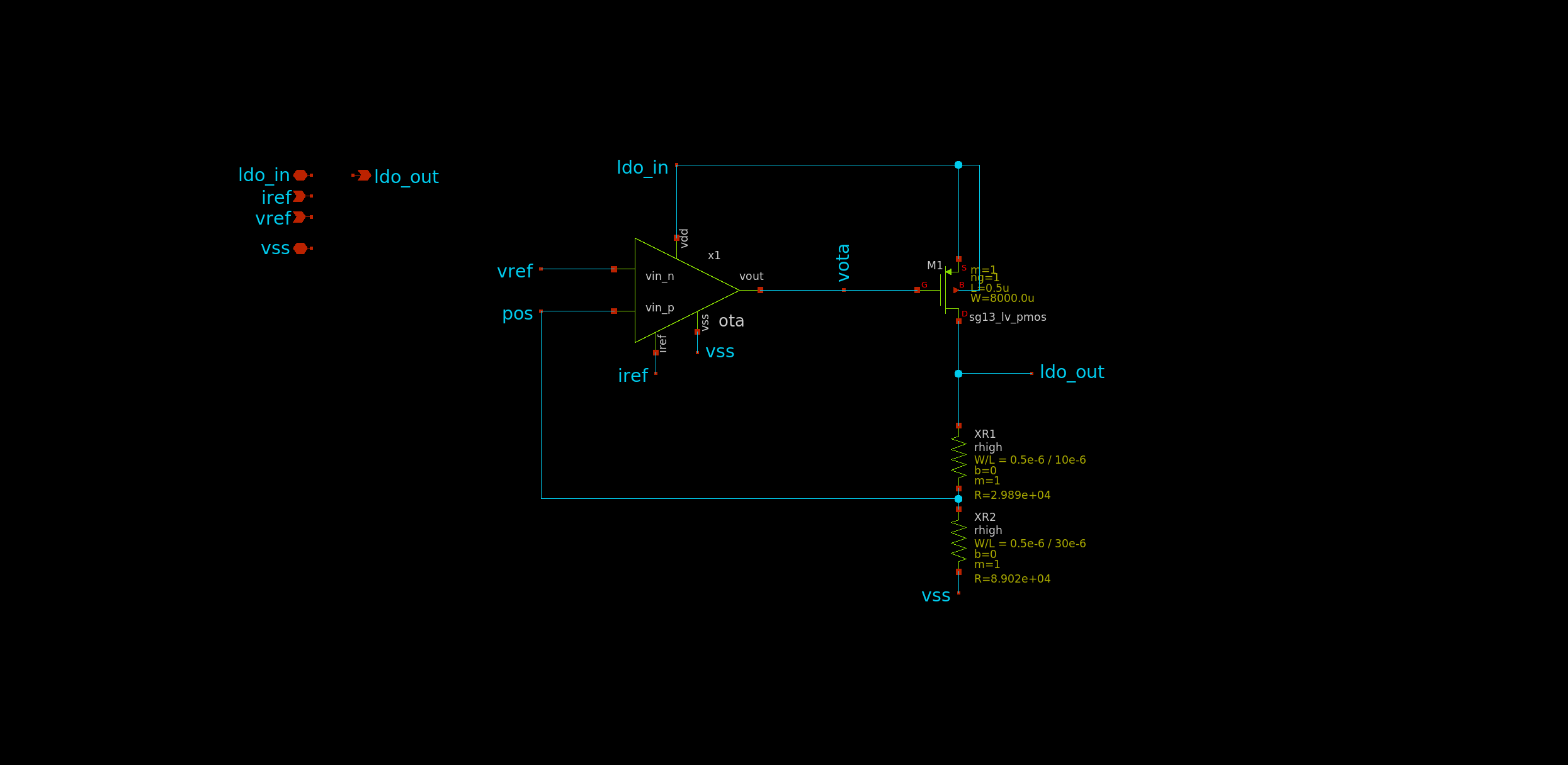
LDO Topology
Aimed Specifications
Parameter |
Value |
|---|---|
Dropout Voltage (mV) |
<250 |
Line Regulation (mV/V) |
<1 |
Load Regulation (mV/mA) |
<0.01 |
Quiscient Current (uA) |
<55 |
Maximum current load (mA) |
100 |
Phase Margin |
>60* |